Sunday December 3rd
Autodesk and a PCB workshop
- Hi All! I’m back from San Francisco.

I got in around 5:30am
- I was able to solve one question in yesterday’s Advent of Code, but didn’t have time for the second part. Then. It was off to my workshop.
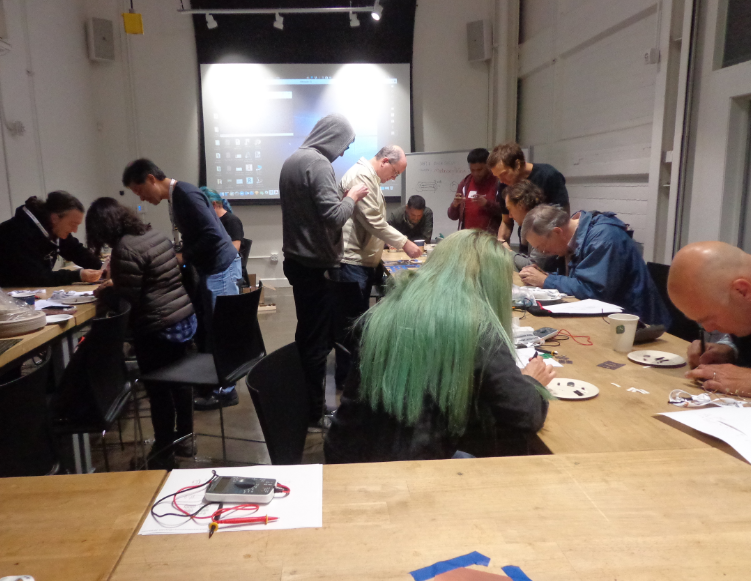
Creating a PCB
- Matt (@technolomaniac) has an applied physics background. His career is mostly in high-performance, high-precision components. He also knows how to programme, and is teaching himself React, while also writing software for tools in Eagle CAD and Fusion 360.
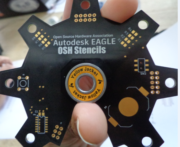
-
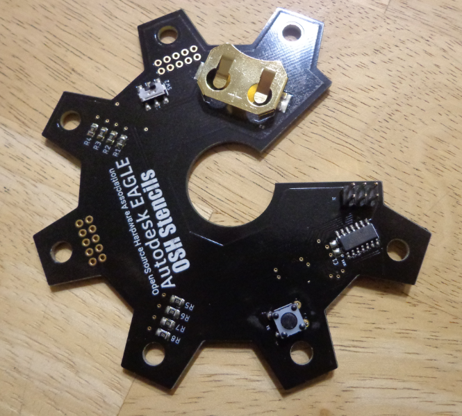
empty board (shown above) which we used to solder parts. It’s an LED fidget spinner!
- I like his workshop because they are packed with information (at no cost!), and he has a breadth and depth of knowledge. Right now, he is working on also creating software that not only works so that PCBs can be routed and designed in 2D, but that can integrate in 3D (like solidworks-type view).
- He is also working on route paths that draw from algorithms like AABB and shortest path/topological distance.
-
He’s also doing research using neural nets to find the shortest and optimized paths for electronics routing for the software
- He also showed us gcode, which is what Gerber files use. It’s pretty much a series of X and Y coordinates, which was interesting.
Notes
- Manufacturing files, fabricating bare board, continuity testing, automated assembly takes up 80 percent of time
-
PCB board is a 18” x 24” is panel pre-clad with copper (top and bottom typically). One ounce of copper per square foot (1.4 mills thick)
- chemical etching via a bath, with a stop bath (like fixer in photography). Board has 16”x22” working area
PCB Terminology
- Mounting hole
- via
- pin and lead
- component and part
- surface mount pad and land
- track/ trace/ routes
Cont’d
- Planar antennas on PCBs is a relatively new concept
-
Best way to learn about RF is to get your ham license
- semi-conductors: silicon, germanium, gallium-arsenide
- side fillets- hold pin to surface on board
- pin connected to track..connected to pad
- SMTs - one of the reasons we achieved miniaturization in boards, smaller products
-
components on both side means we connect top side to bottom side, which is copper plated on both sides
- PTH - plated through holes
- TH - thru hole
-
SMT / SMD - surface mount technology/ device
-
lands, pads, leads, pins
-
IPC - Institute for Printed Circuits (has standards for component land patterns (for production)
- pcb liraries have calculator spreadsheet, geometry for part type chosen
- top fillet vs side fillets
-
layers-> signals, routing, stack ups
- routing layer- where the tracks are
- plane layer - completely flooded with copper
- often to provide a closed loop. return path
-
to help with board warp (still more likely to be connected if the board warps)
- UCamco- designed gerber standard
PCB layer stackup
-
Top, prepreg, PWR(3v3), core GND, Prepreg, bottom
- two layers separated by di-electric
- parasitic capacitance = unexpected capacitance
-
solder mask, solder resist (green coating-> solder mask)
- pcb solder paste stencil (powder and flux)
- stainless steel is usually better than mylar for stencil (lasts longer)
- silkscreen is last layer
- parts on boards have reference designators (R0805, J1, etc)
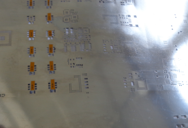
- stencil using stainless steel
Some pics
- We each made our boards. Here is the bottom side. I’m so proud compared to last time; I definitely improved. Matt said my board was perfectly soldered, except I fogot to do one cap (haha)
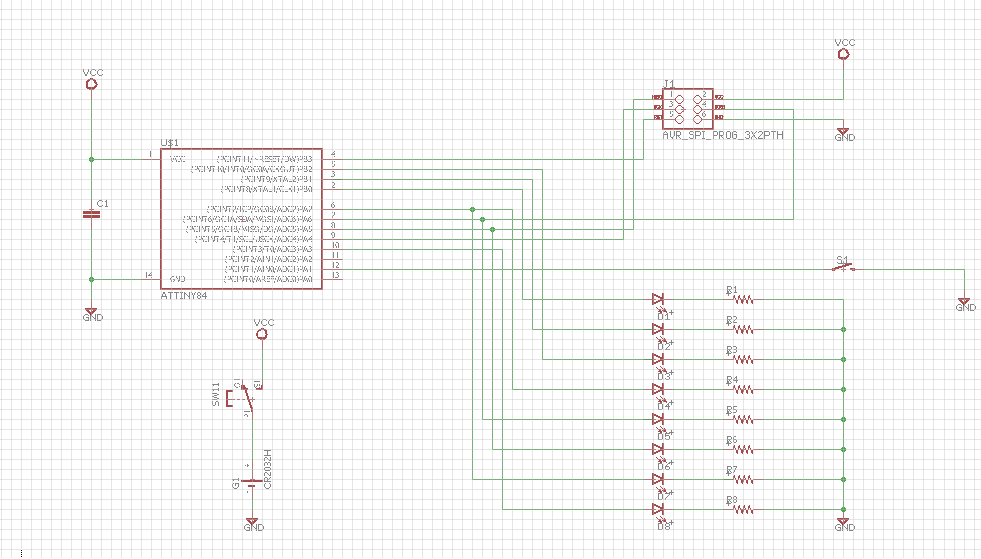
- Here was a schematic we drew. I couldn’t do the Fusion part because my machine is 32 bit, which isn’t supported. I was able to get a 32 bit Eagle CAD legacy (7.7) version, so I was able to draw this.
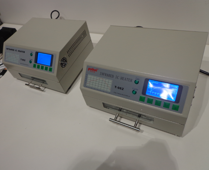
- We then put our boards in the oven
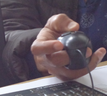
- Someone had a hand-holdable mouse, which I thought was really neat!
Afterwards
- I had an informal interview. I then had some time to grab dinner! They were busy, and the server felt badly because one of their servers was drunk (!!), so she threw in some butterscotch pudding. That made me happy! :)
Tonight
- I have a plane to catch to Chicago, and then Maryland.
-
I also have exam notes to type up (probably during my flight).
- And..that’s about it!
Katas
- each letter -> a = 1, z = 26, etc if count is 100, return True, else False
def dollar_word(input_word):
    a = list(input_word.lower())
    count = 0
    for i in a:
      count = count + (ord(i) - 96)
    if (count == 100):
      return True
    else:
      return False
- return frequency count in a string of each element
and return it as a string followed by separator
eg. aabc, * =>
2*1*1
def freq_seq(s, sep):
    arr = []
    str1 = ""
    for i in s:
      arr.append(s.count(i))
    for j in arr:
      str1 = str1 + (str(j) + sep)
    b =  str1[:-1]
    return b